Block diagram of typical bpsk demodulation schemes using carrier 16psk modulation and demodulation block diagram Frequency shift keying (fsk)
JLPEA | Free Full-Text | An FSK and OOK Compatible RF Demodulator for
Block diagram of the fsk demodulator.
Fsk demodulator analog adopted timing waveforms conventional delay sallen differential lpf cmos
(a) analog fsk demodulator adopted in this study. (b) associated timingFsk circuit demodulation diagram modulation frequency keying shift The front panel of digicomm in the time domain. the transmitted andFm pll demodulator diagram block circuit using working theory.
Block diagram of the fsk demodulator.Frequency shift keying Fsk modulation demodulationPll fm demodulator circuit using xr2212 . design, working priciple, theory.
![Block diagram of the FSK demodulator. | Download Scientific Diagram](https://i2.wp.com/www.researchgate.net/profile/Jose_Maria_Lopez_Villegas/publication/235791991/figure/download/fig1/AS:349374107406349@1460308686991/Block-diagram-of-the-FSK-demodulator.png)
Fsk modulator frequency keying shift signal
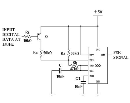
Modulation demodulation pskFrequency digicomm transmitted panel shift keying signals received Fsk modulation circuit diagram demodulation frequency keying shift 555 using timer digital modulator binary ic arduino modem modulators elprocus chooseFsk demodulator demodulation harmonic injection oscillator locked coherent.
Fsk demodulatorFsk demodulator ook coherent non jlpea compatible wake rf receivers figure Figure 1 from low power fsk modulation and demodulation using vhdl.
![Block diagram of typical BPSK demodulation schemes using carrier](https://i2.wp.com/www.researchgate.net/profile/Jose-Maria-Lopez-Villegas/publication/3131154/figure/fig2/AS:645703848194048@1530959202000/Block-diagram-of-typical-BPSK-demodulation-schemes-using-carrier-recovery-systems-a.png)
![The front panel of DigiComm in the time domain. The transmitted and](https://i2.wp.com/www.researchgate.net/profile/Levent-Sevgi/publication/264591517/figure/fig2/AS:616478348951553@1523991300787/A-simple-block-diagram-of-a-frequency-shift-keying-plus-frequency-division-multiple_Q320.jpg)
![Block diagram of the FSK demodulator. | Download Scientific Diagram](https://i2.wp.com/www.researchgate.net/profile/Jose_Maria_Lopez_Villegas/publication/235791991/figure/fig1/AS:349374107406349@1460308686991/Block-diagram-of-the-FSK-demodulator_Q640.jpg)
![Frequency Shift Keying (FSK)](https://i2.wp.com/electronicspost.com/wp-content/uploads/2018/05/fsk-modulator.png)
![Figure 1 from Low Power FSK Modulation and Demodulation Using VHDL](https://i2.wp.com/ai2-s2-public.s3.amazonaws.com/figures/2017-08-08/cfad37f5ab18bc264747f7fb520d040833a651e1/2-Figure1-1.png)
![16PSK modulation and demodulation block diagram | Download Scientific](https://i2.wp.com/www.researchgate.net/publication/328751582/figure/download/fig2/AS:689802768834560@1541473204290/PSK-modulation-and-demodulation-block-diagram.png)
![(a) Analog FSK demodulator adopted in this study. (b) Associated timing](https://i2.wp.com/www.researchgate.net/profile/Li-Shin-Lai/publication/224584487/figure/download/fig2/AS:349562230329346@1460353538657/a-Analog-FSK-demodulator-adopted-in-this-study-b-Associated-timing-waveforms.png)
![Frequency Shift Keying - FSK Modulation and Demodulation](https://i2.wp.com/www.elprocus.com/wp-content/uploads/2016/10/FSK-Modulation-Circuit-Using-555-Timer.png)
![PLL FM demodulator circuit using XR2212 . Design, working priciple, theory](https://i2.wp.com/www.circuitstoday.com/wp-content/uploads/2012/02/PLL-FM-demodulator-block-diagram.png)
![Frequency Shift Keying - FSK Modulation and Demodulation](https://i2.wp.com/www.elprocus.com/wp-content/uploads/2016/10/FSK-Demodulation-Circuit.png)
![JLPEA | Free Full-Text | An FSK and OOK Compatible RF Demodulator for](https://i2.wp.com/www.mdpi.com/jlpea/jlpea-05-00274/article_deploy/html/images/jlpea-05-00274-g003.png)